Designed By Peter C. McNulty, WA1SOV December 20, 1999
With LabView Controls designed by Cristian Craciun, & Peter C. McNulty, April 25, 2000
Theory of Operation
The system arrived at in the design trades yielding the most practical
approach is a design which utilizes a software engine to demodulate different
modes of communication. Doing this provides a standardized hardware platform
that can be used for many different applications, and over a wide bandwidth.
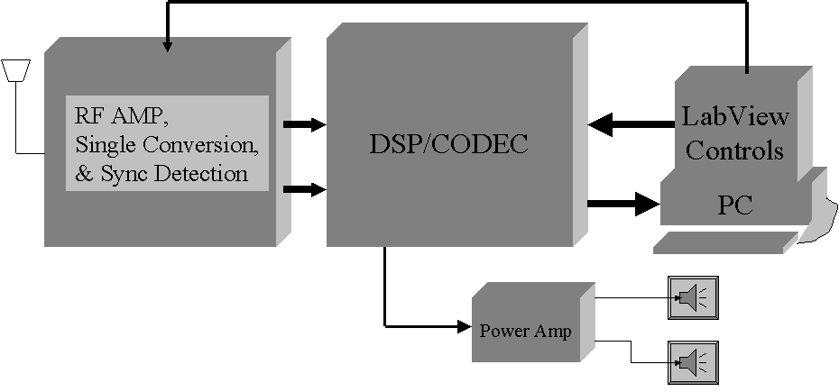
The basic model for this radio is a single conversion synchronous detection
system followed by a CODEC and DSP platform as seen in Figure 3.1. The
analog circuitry is most typically known as a Single Conversion Superheterodyne
Receiver with the addition of a synchronous detection feature.
The Software Radio starts with a high gain, low noise, analog amplifier. The amplifier produces a usable signal, which can then be filtered and detected down stream. Most of the gain is usually apportioned to this amplifier. In this way the system can be said to be "Front End Noise Limited", or in other words produces the best noise floor possible for this design technique. A signal to noise ratio is derived from the system performance parameters for the receiver. From this the amplifier's gain is set to give maximum signal into the mixer input without driving the stage into saturation. The dynamic range is set by the ratio of maximum signal, to the noise floor of the amplifier in use. The noise floor of this amplifier is given in terms of noise figure and is generally supplied by an amplifier's manufacturer.
Other issues to be considered are the Front-End selectivity. Because this amplifier must handle tremendous dynamic ranges, many times a weak signal will be near a relatively strong signal. If the receiver front end does not possess adequate selectivity to reject this
out-of-band signal, then a non-linearity will exist. This problem is
typically called de-sensing a receiver. The way in which this is handled
is to provide adequate bandpass filtering to reject the out-of-band signal.
This filter generally may require tuning depending on the design. Though
the "Front End" is a normal component of a Radio Receiver, it is thought
that it may not be necessary to successfully demonstrate the feasibility
of the Software Radio. It is not planned for this project.
The Mixer stage serves to multiply the incoming signal with an oscillator
running at a frequency selected by the user. This is called the Local Oscillator.
The following illustrates the math involved in this function:
The Signal is represented by:
![]() (2.3)
(2.3)
If the spectral Equation (2.3) is plotted as a function of
frequency, the plot will show that there is a replica of the input signal
er(t),
at the sum and difference of the input frequency of the signal er(t),
and the LO(t). The local oscillator is chosen so the output frequency
will be a standard frequency. This is done because components are made
for specific frequency conversion standards. One of them is 455 KHz and
this is the one that will be worked with in this design. So if a 1 MHz
carrier was present at the input of the mixer, and an output frequency
of the mixer is to be 455 KHz then the L.O. frequency would be adjusted
to be 545 KHz. This would yield products at 1,545 KHz and 455 KHz. A lowpass
or bandpass filter is applied to the output of the mixer to attenuate the
unwanted sideband artifact of the mixing product. A bandpass filter is
generally used with a bandwidth suitable to allow the desired modulation
information to pass. The bandwidth of the filter is mode dependent so it
may be designed to be adjustable.
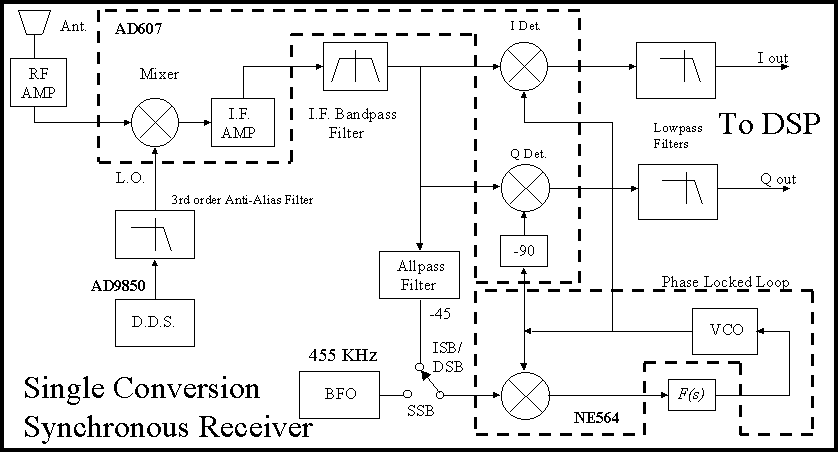
Here the signal has been converted and conditioned to 455 KHz. The function of this stage is to amplify the signal up to a usable level for the detection process. The stage is usually designed to have variable gain so an Automatic Gain Control (AGC) can help control the widely varying levels encountered in radios of this type. Typical AGC circuits work off the detector and measure the signal level out of the detector. This level is then applied to a time constant, and fed back to control the I..F. and Mixer gain stages. In other words, the larger the signal the more feedback to reduce the gain. Under weak signal conditions there may be little or no feedback voltage applied. In this design however, the carrier is recovered with a Phase Locked Loop (PLL) making it undesirable to use conventional AGC. This design incorporates an audio derived AGC which is the average level of the modulation information as detected in the DSP.
I/Q Detectors and Carrier Recovery
The I and Q detectors produce the product of the 455 KHz I.F. signal, and the output a PLL Voltage Controlled Oscillator produce a demodulated signal at the output of the two Product Multipliers. One output is 90 degrees out of phase from the other. The quadrature output arrangement permits the use of phasing techniques to further demodulate these signals. In 1956 Norgaard described the Phasing Method of Single Sideband (SSB) Generation. This method was not to popular when only tubes were available to build hardware because of stability issues. However, with today's technology this technique proves quite efficient in demodulating Single Sideband and Independent Sideband. This technique will be utilized in the Software Engine to perform this signal processing, and is discussed in section 2.5.
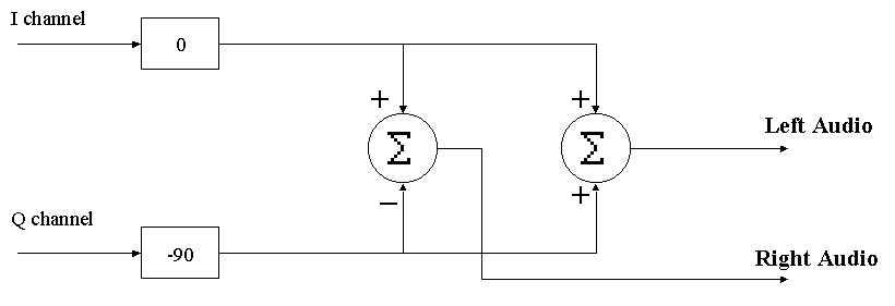
Examining the diagram of Figure 5, the filtered output of the I.F. amplifiers (paragraph 2.3) then looks like the following:
where: s(t) is the modulation information
![]()
![]() (2.6)
(2.6)
where:t is the time constant associated with the single pole low pass filter
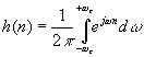
and if this signal is then convolved with the impulse response of a low pass filter as in Figure 5 then the original function s(t) is recovered as seen in (2.6).
The Product Multipliers providing the output must be referenced to a
phase coherent signal however in order for this to work. This is achieved
in the loop formed around the VCO shown at Figure 5. Here the 455 KHz signal
is passed through a hard limiter to remove amplitude components of the
I.F signal. The output of the limiter drives a phase comparator. Here the
error produced is the difference in phase between the 455 KHz I.F. signal
and the VCO output. When these two inputs are exactly in quadrature, the
phase comparator produces no output. Equation 2.7 illustrates why this
happens. When the I.F. is cos(0) = 1 and the sin(0) = 0 then there is no
error to correct the VCO phase and the loop is satisfied. Then the VCO
is said to be in Quadrature to the I.F. signal. This will produce an output
at both Product Multipliers. It is important to consider other conditions
of phase besides at 0. If the phase was 90, 180,or 270, all these conditions
will produce zero error signal. It is important to discriminate between
these.
The Software Engine is an adaptation of a previous design used by one of the authors. The Software running is programmed into an EEPROM, which contains the application specific program to perform a particular demodulation mode.
![]() (2.9)
(2.9)
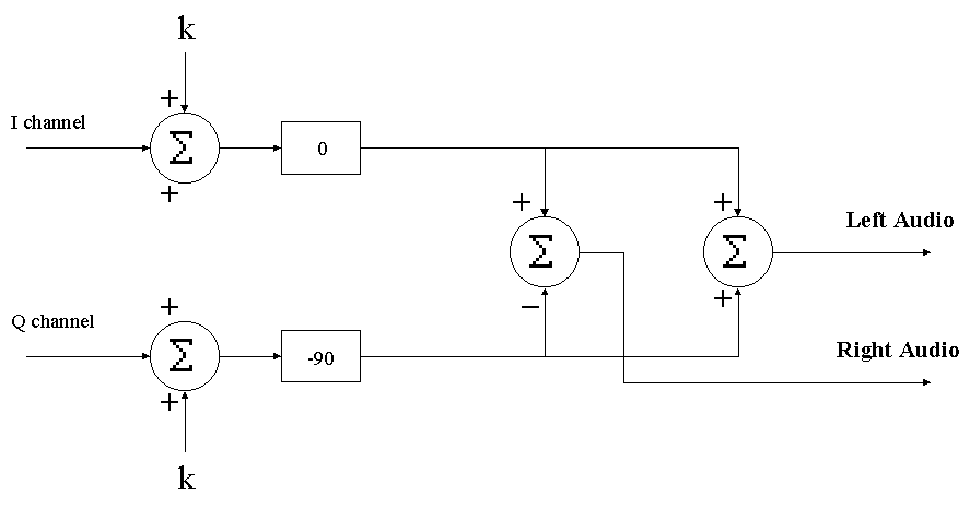
In this system so far only modes with a carrier present have been discussed.
Figure 3.4 shows an additional constant added to the data. This constant
represents the carrier term, and serves to recover the carrier in suppressed
carrier systems, which do not have sufficient carrier to lock the PLL to.
The hardware circuitry of the Software Radio is composed of the receiver Mixer, I.F., and Detector stages shown in Figure 3.1. The DSP, which is a Motorola DSP56002EVM board, a store bought set of PC powered speakers, and the LabPC circuit board which is installed in the PC, provides the interface for Labview.
Analog Mixer/Amplifier, and Quadrature Detectors
An AD607PCB is used for these functions. This unit is capable of operating over very wide bandwidth. For this project the frequency coverage has been set for 500 KHz to 10 MHz. This is well within this chip's operating capability. Figure 4.1 shows the part architecture. This part provides most of the requirements for the analog circuitry of the Software Radio. At the outset, calculations indicated that no additional gain is required. So no R.F. preamplifier is planned. If it is found to be necessary then this will be added to the input of this design. Sections 3.2 through 3.3 cover the description of the function offered by this chip as part of the Theory of Operation.
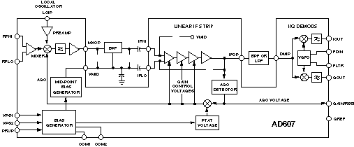
During Breadboard testing it was found that the internal PLL of the AD607 was not adequate for locking to the signals required for communications reception. This was largely due to the fact the internal circuitry does not fully recover the carrier. As a result a PLL was added to the design. This loop is shown in Figure 3.2 and was described in detail in section 3.4. A NE564 was selected for this function and has been built to perform the carrier recovery functions covered in the section 3.4 description.
The Digital Signal Processor is a DSP56002EVM. The EVM is an evaluation module sold by Motorola. The EVM is complete with a 16 bit stereo CODEC (Crystal CS4215) which provides the audio interface to the DSP. The EVM also uses an On Chip Emulator (OnCE) resident on the DSP56002 processor, and is accessed through a dedicated RS232 communication port. The DSP runs at 40 MHz with the in the stock configuration but can be programmed for other speeds up to 80 MHz with the on-chip programmable Phase Locked Loop (PLL). There is 32k of built in static RAM. There are three ports on the DSP itself. Port A is used to read/write memory from the Central Processing unit (CPU). Port B is a host parallel interface. Port C is used to program the CODEC and exchange data with it. This port is a high-speed serial interface.
The analog output from the DSP is sent to a programmable gain audio
amplifier. This consists of an OP270 operational amplifier with a DAC08
used to control the gain of the amplifier. Labview provides an 8 bit output
word used to control the DAC output. This circuit is used for both outputs,
left and right.
The software processing performs to major operations in the Software Radio:
The generic Hilbert Transformer here was designed to implement a 128 tap FIR in phase and 128 tap Quadrature FIR filters. The two legs of the filter are necessary to keep the group delay constant. A 90-degree phase shift is desired out of one of the legs. The filter is developed around a classical Hilbert Transform . The Windowing technique of filter generation was used. The Matlab program developed utilizes the built in Kaiser Window algorithm, which Matlab employs. The development of the Kaiser Window function is well documented in the reference. The filter attenuation, out of band is down over 100 dB and the phase ripple is much less than one degree over the passband of the filter. This implementation of a Hilbert Transformer is a Low Pass. The following is the development of this filter;
![]() for
for ![]() (2.10)
(2.10)
Hilbert Transform Transfer Function
 (2.11)
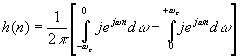 , (2.12)
![]() ,
,
![]() ,
,
So,
 (2.13)
![]() ,
,
![]() , So,
, So,
![]()
The software written for this project was created in Motorola 56000 Assembly Language. A flow diagram of the code can be found in Figure 5.1. There are several initializations that take place upon power up. The filter coefficients are read in from files ISBI_FIR.DAT and ISBQ_FIR.DAT. Next the DSP initializes, and the CODEC Sampling rate, and I/O configuration is set. Finally, the filter loop is initialized setting the beginning conditions for the circular buffer.
The CODEC communicates with the DSP through the Synchronous Serial Interface port. This port must be synchronized with actions being processed in the DSP. As a result there is a Frame Sync loop which synchronizes the program to the data stream (real time audio) coming in. The filter algorithm must be finished before the processor goes back to check for the next data sample. Otherwise, the filter will not be correctly executed. This is where the processor speed becomes important. This is a 20 MIP machine as configured with internal clock running at 40 MHz. MIPS (Mega-instructions per second) in a DSP mean number of multiply-accumulates that occur in one sample. If you are doing fewer MACS (Multiply Accumulate) than 20 MIPS, then the system will work correctly. (In this processor a MAC takes two clock cycles) In this case the requirement is:
![]()
Since 13.284 is less than 20 the filter will function normally in this application. Once frame sync is detected the processor inputs its first data words from the CODEC (I & Q) and stores them in two register. The filter subroutine is then called. The processor has two 24-bit accumulators, which the I sample and the Q sample are processed in separately. The filter coefficients are normalized to less than one so the processor operates in its fixed-point fractional data mode directly.
The following is a description of the DSB, ISB, and SSB modes. The elegance of this design is the ability to facilitate multiple modes with one software implementation. The first thing to happen is, the accumulator is cleared. Then the data state pointer, and the filter coefficient pointers are incremented to n+1 in the circular buffer. Then a loop is executed to increment the state data and coefficient pointers through the entire buffer. So after a pass through, the circular buffer winds up at n sample. Then the buffer is decremented by 1 so the pointer winds up at n-1. This is done so new samples can update the buffer as they come in. Hence the term circular buffer.
After the first pass the I & Q data have been processed so these data can be added to produce the upper sideband. Then the same processed samples are subtracted to produce the lower sideband. This data is then transmitted back to the CODEC for processing through the DAC in the CODEC. The new audio samples appear after this at the Left and Right audio output ports of the CODEC. The program runs continuously since it is a real time filter. In actual operation, DSB (Double Sideband) will appear in common mode on each channel respectively. SSB (Single Sideband) depending whether it is USB (Upper Sideband) or LSB (Lower Sideband) will appear in the Left or Right channels of the CODEC output only. The appropriate sideband can be summed to both channels to reject the opposite sideband. When desiring ISB (Independent Sideband, AM Stereo) reception the left channel will carry the upper sideband and the right channel will carry the lower sideband. Figure 9 illustrates the Software flow executed in this algorithm.
Due to time constraints on this Project the FM and Data modes that were
discussed for this development were not pursued. It was deemed that the
Software Radio could be successfully demonstrated without these additional
features.
EEPROM's are used as the Firmware vehicle. These can be programmed through the EVM. Each mode will be provided via a different Firmware chip. This was one of the original marketing features surfaced early on in the development of this Software Radio. There are separate modules for the modes AM, ISB, DSB, SSB, and CW will contain their own modules. Separate programs will be available for loading through the OnCE (On Chip Emulator) port for debugging purposes.
References:
Harris Broadcast Division, Planning a Future-Proof AM Transmission Airchain, Digital Radio
http://www.broadcast.harris.com/the-key/c24.pdf
The ARRL Handbook, 1994, Seventy First Edition, Page 12-9, Superheterodyne Receivers
Modulation, Noise, and Spectral Analysis, Phillip F. Panter, Ph.D.Copyright 1965 McGraw-Hill
pg. 209 equation 6-7.
Norgaard, D.E.: The Phase-Shift Method of Single-Sideband Signal Generation, Proc. IRE December, 1956
AM Stereo Diversity Modulation Exciter, Peter C. McNulty, August 2, 1999, Fairfield University
Analog Devices, Analog Dialog, vol. 29-2, AD607 Architecture, pg. 2
Excerpt from reference iv, pg. 7, Digital Signal Processor
Oppenheim & Schafer, Digital Signal Processing, Prentice-Hall 1975,
ISBN 0-13-214635-5, Section 7.4.1, page 361.
QST, April 1998, Frohne, R2 Receiver
http://www.analog.com/pdf/AD9850_e.pdf
http://www.ni.com/pdf/manuals/320502b.pdf
AD9850_e.pdf available at http://www.analog.com/
AD607.PDF available at http://www.analog.com/
NE564.PDF available at http://www-us2.semiconductors.philips.com/index.html